The prevalence of electronic devices has transformed life in the 21st century. At the heart of these devices is the movement of electrons across materials. Scientists today continue to discover new ways to manipulate and move electrons in a quest for making faster and better functioning devices.
Scientists from the Femtosecond Spectroscopy Unit led by Prof. Keshav Dani at the Okinawa Institute of Science and Technology Graduate University (OIST) have demonstrated a new mechanism that can potentially allow the control of electrons on the nanometer (10-9 of a meter) spatial scale and femtosecond (10-15 of a second) temporal scales using light. The study has been published in the journal Science Advances.
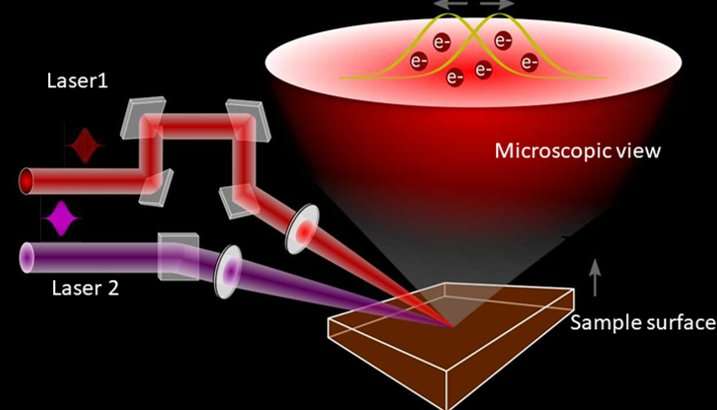
When a voltage is applied across semiconducting materials, an electric field is generated that directs the flow of electrons through the materials. Dr. E Laine Wong, a recent Ph.D. graduate at OIST, and her colleagues have used a physical phenomenon called surface photovoltage effect, to induce electric fields on the material surface allowing them to. Surface photovoltage effect is an effect where the surface potential of the materials can be varied by changing the light intensity. “By making use of the nonuniform intensity profile of a laser beam, we manipulate the local surface potentials to create a spatially varying electric field within the photoexcitation spot. This allows us to control electron flow within the optical spot,” says E Laine.
Using a combination of femtosecond spectroscopy with electron microscopy techniques, E Laine and her colleagues made a movie of the flow of electrons on femtosecond timescales. Typically, in femtosecond spectroscopy, an ultrafast laser beam known as the ‘pump’ is first used to excite the electrons in the sample. A second ultrafast laser beam known as the ‘probe’ is then shone upon the sample to track the evolution of the excited electrons. This technique, also known as pump-probe spectroscopy, has allowed the scientists to study the dynamics of the excited electrons at a very short time scale. The combination of an electron microscope then further provides the scientists with the spatial resolution required to directly image the movement of the excited electrons even within the small area of the laser beam spot. “The combination of these two methods with both high spatial and temporal resolutions has allowed us to record a movie of the electrons being directed to flow in opposite directions,” says E Laine.
The findings of the study are also promising to control the movement of electrons beyond the resolution limit of light by utilizing the spatial intensity variations of the laser beam within the focal spot. The mechanism could therefore be potentially used to operate nanoscale electronic circuits. Prof. Dani and his team are now working towards building a functional nanoscale ultrafast device based on this newfound mechanism.
Find your dream job in the space industry. Check our Space Job Board »
Provided by:
Okinawa Institute of Science and Technology
More information:
E Laine Wong et al. Pulling apart photoexcited electrons by photoinducing an in-plane surface electric field. Science Advances (2018). DOI: 10.1126/sciadv.aat9722
Image:
Study demonstrates new mechanism for developing electronic devices
Scientists combined femtosecond spectroscopy and electron microscopy techniques to observe the motion of the electrons in both short time and spatial scales.
Credit: Femtosecond Spectroscopy Unit, OIST
